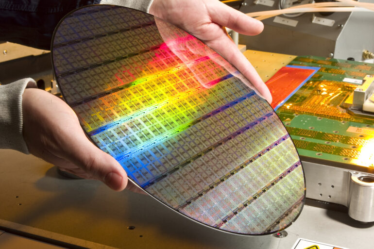
Used for machine demonstration, material screening, and process development, test wafers provide a plethora of benefits as opposed to popular product wafers. These testers are manufactured at an affordable price and, based on the composition of testers, can provide related advantages to their users.
From patterned silicon wafers to glass and SOS wafers, these testers are used during semiconductor device fabrication to assess any functional defects present. You can find a variety of test wafers even available in customized designs for different applications.
Here is a comprehensive guide to testing wafers and various applications of it.
Different Types Of Test Wafers
1. Silicon Wafers

A popular and widely used material, silicon wafers are used in micromechanical and electronic devices. Silicon testers possess various parameters, making them one of the most suitable components for wafer selection.
Diameters of silicon test wafers can range from 2″- 12″, with 4″, 6″, and 8 “most commonly used for market purposes. Depending upon the quality of silicon wafers, these testers can be classified into Prime, Test, and Reclaimed, with Prime being of the optimum quality and Reclaimed being created from previous patterning or processing. Prime wafers have the highest quality of cleanliness, flatness, and polish. Some subsets of silicon wafers also include oxide and nitride wafers.
2. Glass Wafers

When you wish to make the substrate transparent, glass wafers are used in such situations. The materials usually used for glass wafers are crystal quartz, borosilicate, fused silica, and fused quartz. The grade of the glass wafers usually depends on the manufacturer’s specifications.
3. SOS Wafers
SOS wafers are created upon a silicon layer grown over a sapphire substrate. These test wafers are usually used in appliances where the excellent insulation properties of sapphire are required. For example, to shield the appliance from stray radiation-induced currents.
Manufacturing Process Of Test Wafers

The test wafers must be manufactured perfectly to ensure no compromise on the function.
The steps usually incorporated in the manufacturing process of test wafers are as follows.
1. Silicon Wafers
Our earth’s crust consists of 30% silicon, and when silica sand mixed with carbon is heated at a temperature beyond 2000 degrees in an electrical furnace, silicon gets separated with 99% purity.
To ensure the optimum functionality of the silicon testers is guaranteed, the 99% pure silicon testers are further subjected to purification. The process usually contains a variety of steps, including some complex terminologies. Still, the process can be summarized as creating a product that is 99.999% pure, made upon grounding the silicon into a fine powder, mixing it with HCl, and turning it into a liquid by heating.
The next step involves melting the silicon crystals over a quartz crucible, thus creating a silicon ingot free from the above-said crystalline structures. Once the silicon ingot is formed, steps like slicing, dicing, and smoothing ensure the test wafer meets the desired criteria.
2. Glass Wafers
First, the appropriate material is chosen for glass testers, usually crystal quartz, borosilicate, fused silica, and fused quartz. Borosilicate is among the most affordable and widely used materials for tester manufacture.
Once the material is selected, using advanced tools, the desired shape of the tester is created and then perfectly designed to match the machine’s specifications. Other processes like lapping, polishing, and inspection are included to maintain all desired standards.
3. SOS Wafers
In the case of SOS testers, a thin layer of silicon, through a hetero-epitaxial process, is grown on sapphire. Essentially, high-quality sapphire crystals are grown, and silicon is deposited on the crystals through the decomposition of SiH4 (Silane) gas.
After manufacturing the testers, the cleaning process holds vital significance. Tiny particles can disrupt the electrical flow, so effective precautions are taken to ensure the cleaning process is not compromised. Manufacturers must wear specialized gear, and the process takes place in a clean room to ensure optimum quality.
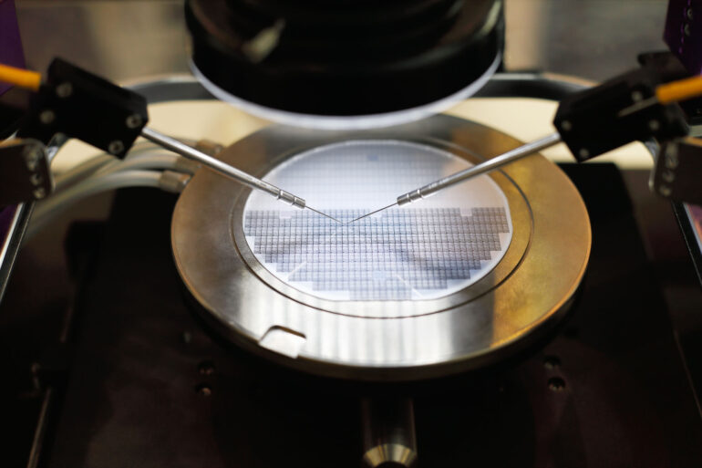
Once the test wafer is manufactured, specialized tests are held to ensure the wafers meet the required specificity. These tests are usually conducted through computer-controlled probes, and once the wafer passes all the tests, the manufacturer can distribute it in the market. However, if it fails to meet the criteria, the wafers are rejected immediately.
How Are The Wafers Used?

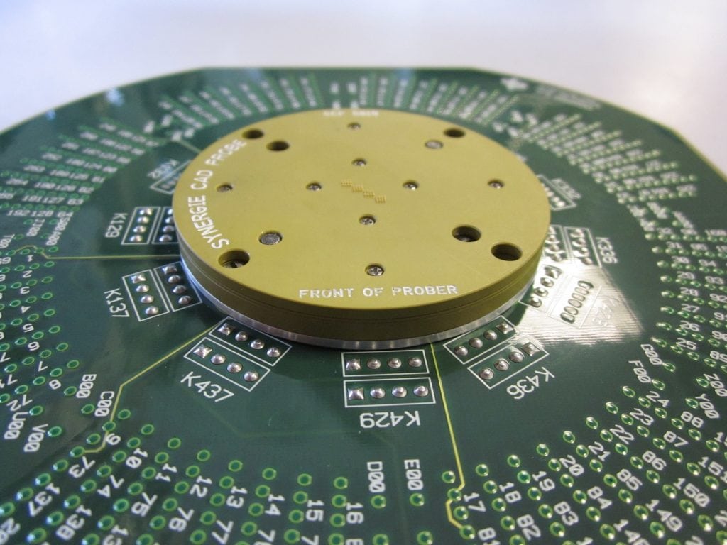
During electrical testing, the testers transmit signals through probe cards or needles to ensure signal leakage and electrical noise can be detected.
Silicon testers are popularly used during material screening, where contact silicon chips in pairs are used to establish a daisy chain, which helps determine the interconnect’s contact resistance. These testers are also used to demonstrate the capability of the machine. Silicon testers can be used in a variety of devices. It also operates on relatively low voltage. No heat is produced upon using silicon test wafers, and one also does not have to hear a humming sound from the machine.
Glass wafers also provide similar advantages. One can observe less electrical loss, better thermal expansion, and increased stiffness. However, glass testers can be costly and difficult to manufacture compared to silicon test wafers.
SOS testers have also become increasingly popular and are specially used in tablets and smartphones. These wafers provide premium pressure transmissions and temperature sensory quality that has exponentially boosted their usage in the technological world.
Both glass and SOS testers have faced quite a challenge in the early market. Still, with the increase of complicated technological devices and the requirement of sophisticated components, these testers will be used more widely in the future.
Bottom Line
Test testers have established their cruciality in the market. Manufacturers have to undergo various steps to maintain the optimum quality according to wafer criteria. As a consumer, you should conduct thorough research to make the final decision. Always choose from a reputable source. You can also search about the different types of test wafers now available in the market and choose the one that works best for your needs. Also, look at the consumer reviews on the website before making the final decision.


